PowerPoint PPT presentation. VLSI Systems Design Design Rules for CMOS Lecture 7.
Vlsi Design Cmos Layout Ppt Download
Static C omplementary MOS Circuits.
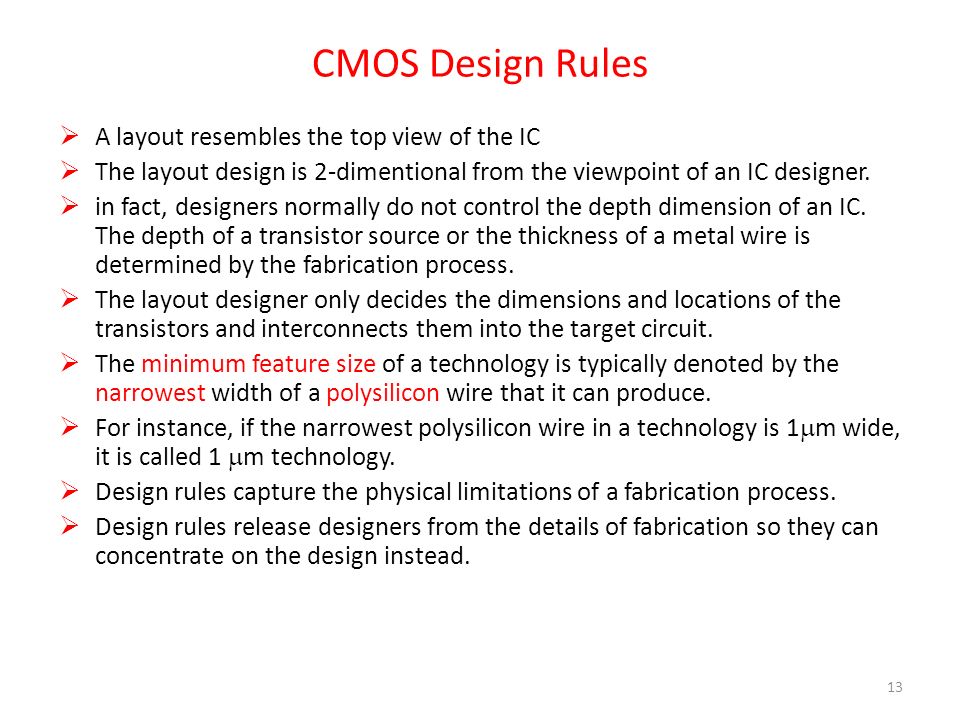
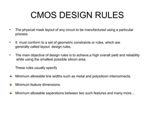
. All widths spacing and distances. VDD and GND should abut standard height Adjacent gates should satisfy design rules. CMOS Layout and Design Rules It is the design responsibility to determine the geometry of the various masks required during processing.
University of Puerto Rico at Mayagüez. PowerPoint PPT presentation free to view. I These rules are the designers interface to the fabrication process.
Valerio Re - INFN. Define cmos design rules - PowerPoint PPT Presentation. Introduction to CMOS VLSI Design Circuits Layout Outline CMOS Gate Design Pass Transistors CMOS Latches Flip-Flops Standard Cell Layouts Stick Diagrams CMOS Gate Design Activity.
INFN WP3 CMOS ASICs for 3D. Structure of CMOS CMOS Gates and Layout Delay Power. Introduction to CMOS VLSI Design Lecture 1.
CMOS Stick Diagrams NOR. CMOS Formation - P diffusion 5. Layout and Cross Section - NMOS 8.
CMOS Layout Example 6. In these processes the minimum poly length is 1µm and 05µm respectively. CMOS VLSI DESIGN RIT PROCESSES At RIT we use the Sub-CMOS and ADV-CMOS processes for most designs.
Design rules I The geometric design rules are a contract between the foundry and the designer. The process of defining the. Vlsi Design Cmos Layout Ppt Download CMOS recommends blocking two or more lines of.
Cmos design rules the physical mask layout of any circuit to be manufactured using a. Design Rules Allow for a ready. Electrical and Computer Engineering Department.
Lambda Based Rules 9. Cross-Section of CMOS Technology Design Rules Interface. Kasin Vichienchom kvkasinkmitlacth Lecture4.
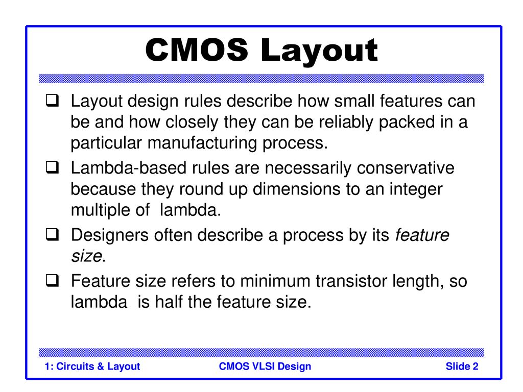
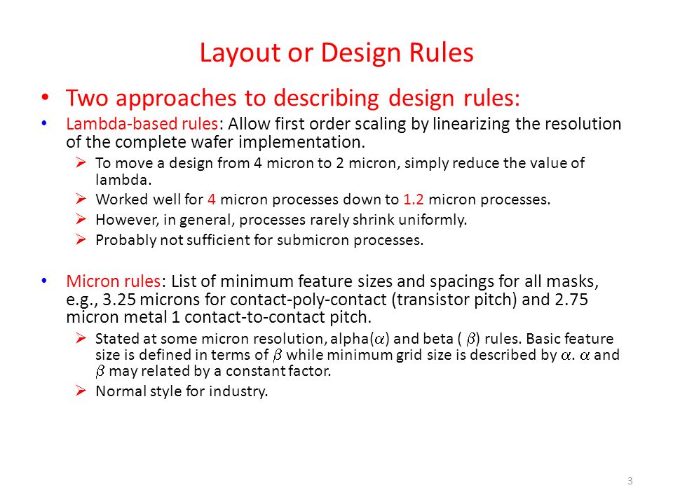
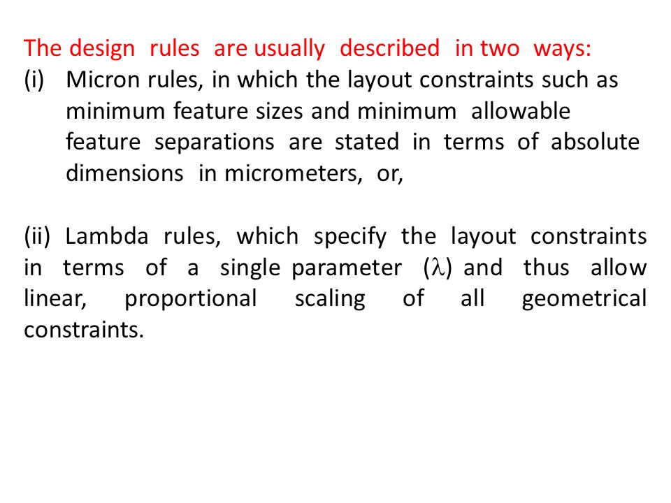
Lambda-based Design Rules Lambda design rules are based on a reference metric λthat has units of um. Design Rules Jan M. I They guarantee that the.
List of Rules to be Considered 7. Rabaey Cross-Section of CMOS Technology Design Rules Interface between designer and process engineer Guidelines for constructing process masks Unit dimension. Design Rules - Free download as Powerpoint Presentation ppt PDF File pdf Text File txt or view presentation slides online.
WP3 AIDA meeting CERN February 16 2011. ELECTRONICS AND COMMUNICATION ENGINEERING Course Code. INFN WP3 CMOS ASICs for 3D.
Lecture 3 CMOS Layout and Design Rules CMOS Layout and Design Rules It is the design responsibility to determine the geometry of the various masks required during.
Layout Design Rules 2 Introduction Layout Rules Is Also Referred As Design Rules It Is Considered As A Prescription For Preparing Photomasks Ppt Download
Purpose Of Design Rules Ppt Video Online Download

Layout Stick Diagram Design Rules

Design Rules Ee213 Vlsi Design Ppt Video Online Download
Layout Design Rules 2 Introduction Layout Rules Is Also Referred As Design Rules It Is Considered As A Prescription For Preparing Photomasks Ppt Download

Layout Stick Diagram Design Rules
Design Rules For Nmos And Cmos
Cmos Design Rule
0 comments
Post a Comment